
High-density ferroelectric topological nanodomains (~200 Gbit/inch2) and reversible switching of their resistive states in the external electric field were achieved by integrating perovskite oxide ferroelectric/dielectric freestanding bilayer on silicon substrates.
This is reported by an article in the latest issue of Nature with the title “High-density switchable skyrmion-like polar nanodomains integrated on silicon” (DOI: 10.1038/s41586-021-04338-w).
The achievement was made through close cooperation between Professor Nie Yuefeng’s and Professor Wu Di’s research teams from the College of Engineering and Applied Sciences at Nanjing University and Professor Pan Xiaoqing’s team from University of California, Irvine.
The successful integration of high-density, rewritable ferroelectric topological nanodomains on silicon shows promising potential for new high-density non-volatile memory using novel oxide polar topological structure.
In recent years, many novel non-trivial polar topological domain structures have been reported theoretically and experimentally in ferroelectric perovskite oxide thin films, superlattices and other systems, including flux-closure domains, vortices, polar bubble domains, polar skyrmions and merons, and exhibit exotic physical properties (such as enhanced conductivity, negative capacitance, etc.). By applying these properties, it is expected to develop new devices such as ferroelectric transistors and memory devices.
Nevertheless, due to the incompatibility of the currently mature process of complementary metal oxide semiconductor (CMOS) with the growing of high-quality perovskite oxide thin films, it is difficult to combine a variety of polar topological domains with the next-generation electronic devices.
In essence, the formation of polar topological domain structures is a result of delicate competition and balance among elastic energy, electrostatic energy and gradient energy. Thus, a special design for material structure, mainly acquired on single-crystal oxide substrates, is needed. Whether the integration on silicon can be realized remains as an important scientific issue.
To integrate perovskite oxide with semiconductor, Professor Nie’s team attempted to fabricate high-quality freestanding ferroelectric thin films and transfer these independent function units to semiconductor substrates.
In their early work, the team resolved the technical issue of in-situ monitoring and growth of oxide films and interfaces at the atomic-layer level by developing Oxide-MBE technique and successfully grew a series of high-quality freestanding perovskite ferroelectric thin that are controllable at the unit-cell level, such as BiFeO3 and PbTiO3.
In this research, the team transferred the freestanding PbTiO3/SrTiO3 (PTO/STO) ferroelectric/dielectric thin films to the silicon substrate. After systematic investigation, a balance has been achieved between elastic energy and electrostatic energy in the freestanding bilayer structure with a specific thickness ratio, thus resulting in high-density polar topological domains and modulation of their resistance.
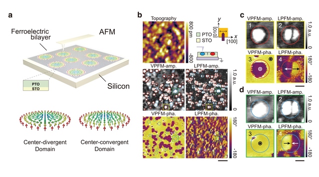
Fig. 1. High-density ferroelectric nanodomains in a PTO20/STO10 bilayer. (a) Schematic description of the release and transfer process of oxide membranes. (b)Topography, VPFM amplitude, VPFM phase, LPFM amplitude and LPFM phase images for the freestanding bilayer. (c, d) Zoomed-in images for center-divergent nanodomain (c) and center-convergent nanodomain (d).
In cooperation with Professor Wu’s and Professor Pan’s teams, Nie’s team detected two types (center-divergent and center-convergent) of high-density (~200 Gbit/inch2) polar nanodomain in the PTO/STO bilayer by using vector piezoelectric force microscope (PFM) and scanning transmission electron microscopy (STEM) (see Fig. 1).
The center-divergent nanodomains show Néel-type polar skyrmion-like structure, while the center-convergent ones only present the inversion of the in-plane polarization.
Meanwhile, Professor Laurent Bellaiche, of University of Arkansas, and Professor Yang Yurong, of Nanjing University, proved through effective Hamiltonian model simulations that the above-mentioned two complex polar topological structures can stably exist in the PTO/STO bilayers.
Additionally, they also found that the two topological nanodomain types are switchable in an external electric field, with reversible switching between high and low resistive states (see Fig. 2).
The ‘on’ and ‘off’ states can be controlled by switching the type of nanodomains, thus providing the opportunity to develop high-density, energy-efficient and non-volatile ferroelectric memory devices.
Compared to the previous multilayer ferroelectric skyrmion topological structure observed in the ferroelectric oxide superlattice, the single-layer polar topological domain in the ferroelectric/dielectric bilayer structure in this research can effectively avoid interaction between multiple layers of topological domains and can make it easier to switch each individual nanodomain by an external electric field, allowing the effectively, energy-saving ‘read’ and ‘write’ operations.
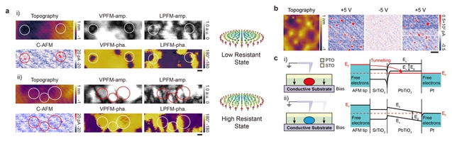
Fig. 2. Resistive behaviours of the polar nanodomains integrated on silicon. (a) Topography, VPFM and LPFM images, and CAFM current maps collected at the same area after a +5-V scan (i) and a −5-V scan (ii); (b) Reversible switching between the low-resistive, center-divergent and high-resistive, center-convergent states by +5-V and −5-V bias voltage; (c) Schematic band diagram of the two different types of topological structure.
One of the referees commented that “the idea and its practical realization to create a new type of Si-integrated resistive memory on the field-controllable domain walls with high-density (>200 Gbit/inch2) is very promising for memory applications of topological polar structures”.
The high-density, rewritable polar topological structure can be successfully integrated on silicon and can remain stable after the lithography process, showing the preliminary possibility of combining abundant oxide polar topological structures with traditional semiconductor process to develop new, energy-efficient, and high-performance electronic devices.
Meanwhile, it is noteworthy that there is still a long way to practical application, with a range of important issues remaining to be solved.
First, there is still a huge challenge to realizing the growth and transfer of wafer-sized large-area high-quality freestanding oxide thin films.
Second, the current ‘read’ and ‘write’ voltages are relatively high. Further structural optimization is required to reduce the voltages so as to meet the energy-efficient, non-volatile reading and writing requirement of commercial memory devices.
Third, exploration is still needed to see whether the polar topological structures can be made into array ones and whether these structures can still exist with top and bottom electrodes.
The solution of these difficulties and the attempt to integrate more novel polar topological structures on semiconductor substrates will promote the application of polar topological structures to the next-generation electronic devices and deserve further investigation.
Han Lu, a doctoral student from the College of Engineering and Applied Sciences of Nanjing University is the first author of the article, with the joint corresponding authors being Professors Nie Yuefeng and Wu Di from Nanjing University and Professor Pan Xiaoqing from UC Irvine.
Professor Chen Yanfeng from Nanjing University offered significant guidance to the research. Professor Laurent Bellaiche from University of Arkansas and Professor Yang Yurong from Nanjing University provided important theoretical support.

